- 您现在的位置:买卖IC网 > Sheet目录1990 > BH2228FV-E2 (Rohm Semiconductor)IC DAC 8BIT 6-CHAN SSOP-B14
BH2227FV, BH2228FV
Technical Note
4/8
www.rohm.com
2011.08 - Rev.B
2011 ROHM Co., Ltd. All rights reserved.
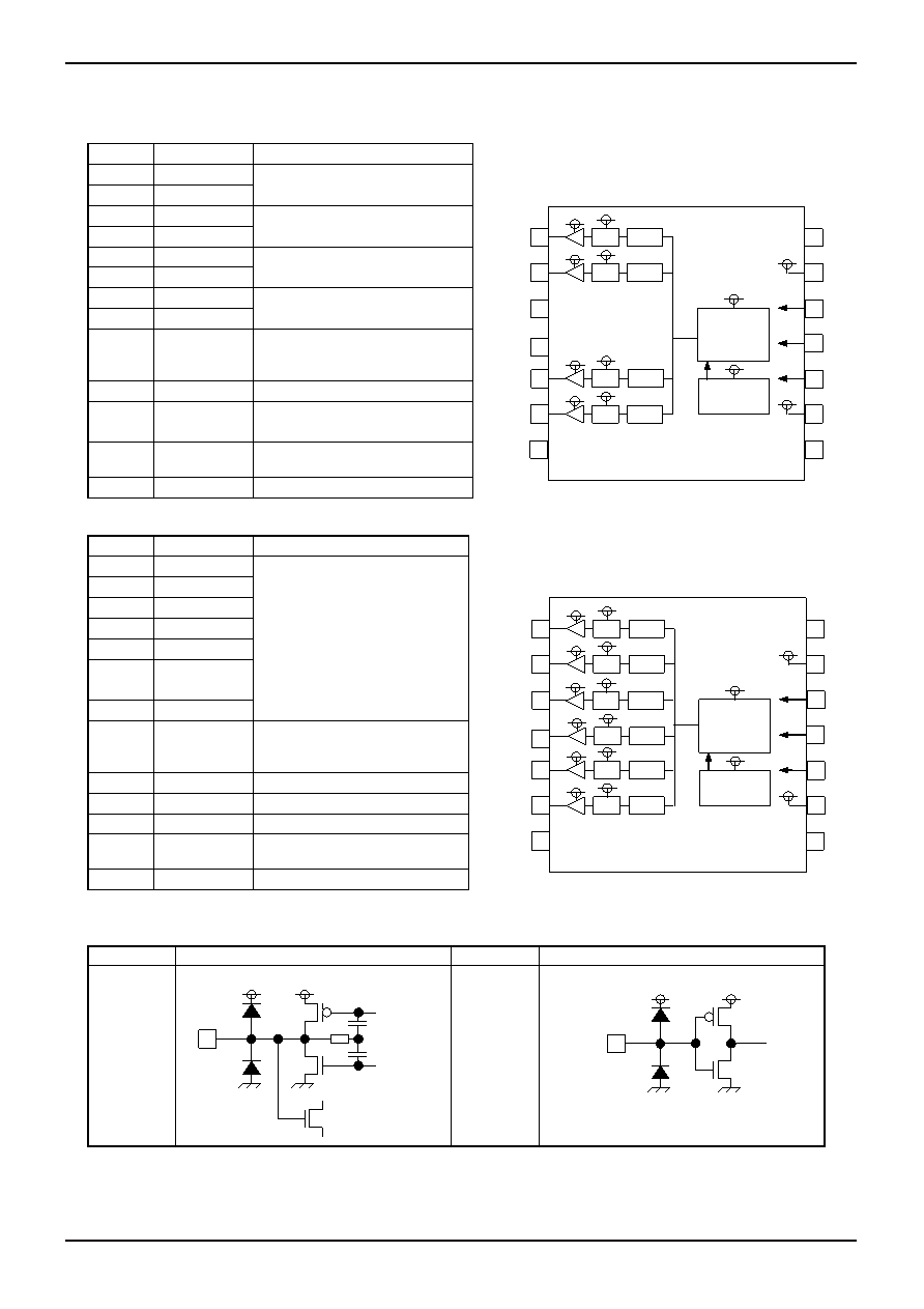
●Terminal Description / Block Diagrams
(BH2227FV)
Terminal Terminal name
Function
1
AO1
Analog output terminal
2
AO2
3
TESTMONI1
Test terminal
(OPEN at normal use)
4
TESTMONI2
5
AO3
Analog output terminal
6
AO4
7
NC
Internally not connected yet
8
NC
9
VDD
Power source terminal
(AO3, 4 full scale voltage
use in common)
10
CSB
Chip select signal input terminal
11
CLK
Serial clock input terminal
12
DI
Serial data input terminal
13
VFS
AO1,2 full scale
Voltage setting terminal
14
VSS
Ground terminal
Fig.2
(BH2228FV)
Terminal Terminal name
Function
1
AO1
Analog output terminal
2
AO2
3
AO3
4
AO4
5
AO5
6
AO6
7
NC
Internally not connected yet
8
NC
9
VDD
Power source terminal
(AO4~6 full scale voltage use
in common)
10
CSB
Chip select signal input terminal
11
CLK
Serial clock input terminal
12
DI
Serial data input terminal
13
VFS
AO1,2,3 full scale
Voltage setting terminal
14
VSS
Ground terminal
Fig.3
●Equivalent Circuits
Terminal
Equivalent circuit
Terminal
Equivalent circuit
AO1
AO2
AO3
AO4
AO5
AO6
DI
CLK
CSB
Fig.4 Equivalent circuit
AO3
AO4
2
AO2
Serial
Interface
VDD
PowerOn
Reset
VDD
R2R
REG
VFS
VDD
1
AO1
5
AO5
6
AO6
7
NC
R2R
REG
VFS
VDD
R2R
REG
VDD
R2R
REG
VDD
14 VSS
13
VFS
12
DI
11
CLK
10 CSB
9
VDD
8
NC
4
VFS
VDD
3
R2R
REG
VFS
VDD
R2R
REG
VDD
VSS
VDD
VSS
VDD
6
TEST
MONI1
TEST
MONI2
2
AO2
Serial
Interface
PowerOn
Reset
R2R
REG
VFS
VDD
1
AO1
5
AO3
AO4
7
NC
R2R
REG
VFS
VDD
R2R
REG
VDD
R2R
REG
VDD
14 VSS
13 VFS
12 DI
11 CLK
10 CSB
9 VDD
8 NC
4
3
发布紧急采购,3分钟左右您将得到回复。
相关PDF资料
BQ4285EP
IC RTC W/114X8 NVSRAM 24-DIP
BQ4847YMT
IC RTC W/NVSRAM CONTROL T-MOD
BU2280FV-E2
IC CLOCK GEN DVD-VIDEO SSOP-B24
BU2363FV-E2
IC CLOCK GEN DVD-VIDEO SSOP-B16
BU2365FV-E2
IC CLOCK GEN W/VCXO SSOP-B24
BU2505FV-E2
IC DAC 10BIT 10-CHAN SSOP-B20
BU2508FV-E2
IC DAC 10BIT 4-CHAN SSOP14
BU3076HFV-TR
IC CLOCK GEN 1CH HVSOF6
相关代理商/技术参数
BH223
制造商:ADAM-TECH 制造商全称:Adam Technologies, Inc. 功能描述:BATTERY HOLDERS & SNAPS AA, AAA, C, D & COIN CELL
BH-22-3
制造商:ADAM-TECH 制造商全称:Adam Technologies, Inc. 功能描述:BATTERY HOLDERS D, 9V SINGLE & MULTIPLE CELLS
BH223-L
功能描述:HOLDER CR223A W/SOLDER LUGS RoHS:是 类别:电池产品 >> 电池座,夹,触点 系列:- 标准包装:100 系列:- 电池类型,功能:圆柱形,触点(单) 样式:触点弹簧(线圈) 电池大小:多重 单元数:- 电池系列:- 安装类型:自定义 端接类型:- 板上方高度:- 工作温度:- 配用:P670-ND - BATTERY 1.5V ALKALINE AAA 4 PACKP671-ND - BATTERY 1.5V ALKALINE AA 4 PACKP672-ND - BATTERY 1.5V ALKALINE AAA 2 PACKP673-ND - BATTERY 1.5V ALKALINE AA 2 PACKP674-ND - BATTERY 1.5V ALKALINE AAAP675-ND - BATTERY 1.5V ALKALINE AATL-4903-ND - BATT LTH AA 3.6VLR03XWA/C-ND - BATT IND ALKALINE AAA SIZELR6XWA/C-ND - BATT IND ALKALINE AA SIZEP649-ND - BATTERY IND ALKALINE AAA更多... 其它名称:211K
BH223-X2-411
功能描述:HOLDR BATT 2-CRP2 OR 223A W/CONN RoHS:是 类别:电池产品 >> 电池座,夹,触点 系列:- 标准包装:100 系列:- 电池类型,功能:圆柱形,触点(单) 样式:触点弹簧(线圈) 电池大小:多重 单元数:- 电池系列:- 安装类型:自定义 端接类型:- 板上方高度:- 工作温度:- 配用:P670-ND - BATTERY 1.5V ALKALINE AAA 4 PACKP671-ND - BATTERY 1.5V ALKALINE AA 4 PACKP672-ND - BATTERY 1.5V ALKALINE AAA 2 PACKP673-ND - BATTERY 1.5V ALKALINE AA 2 PACKP674-ND - BATTERY 1.5V ALKALINE AAAP675-ND - BATTERY 1.5V ALKALINE AATL-4903-ND - BATT LTH AA 3.6VLR03XWA/C-ND - BATT IND ALKALINE AAA SIZELR6XWA/C-ND - BATT IND ALKALINE AA SIZEP649-ND - BATTERY IND ALKALINE AAA更多... 其它名称:211K
BH223-X2-W
功能描述:HOLDER 2 DL223A 12V 6" WIRE LEAD RoHS:是 类别:电池产品 >> 电池座,夹,触点 系列:- 标准包装:100 系列:- 电池类型,功能:圆柱形,触点(单) 样式:触点弹簧(线圈) 电池大小:多重 单元数:- 电池系列:- 安装类型:自定义 端接类型:- 板上方高度:- 工作温度:- 配用:P670-ND - BATTERY 1.5V ALKALINE AAA 4 PACKP671-ND - BATTERY 1.5V ALKALINE AA 4 PACKP672-ND - BATTERY 1.5V ALKALINE AAA 2 PACKP673-ND - BATTERY 1.5V ALKALINE AA 2 PACKP674-ND - BATTERY 1.5V ALKALINE AAAP675-ND - BATTERY 1.5V ALKALINE AATL-4903-ND - BATT LTH AA 3.6VLR03XWA/C-ND - BATT IND ALKALINE AAA SIZELR6XWA/C-ND - BATT IND ALKALINE AA SIZEP649-ND - BATTERY IND ALKALINE AAA更多... 其它名称:211K
BH224
制造商:ADAM-TECH 制造商全称:Adam Technologies, Inc. 功能描述:BATTERY HOLDERS & SNAPS AA, AAA, C, D & COIN CELL
BH225
制造商:ADAM-TECH 制造商全称:Adam Technologies, Inc. 功能描述:BATTERY HOLDERS & SNAPS AA, AAA, C, D & COIN CELL
BH22834E-30
制造商: 功能描述: 制造商:undefined 功能描述: